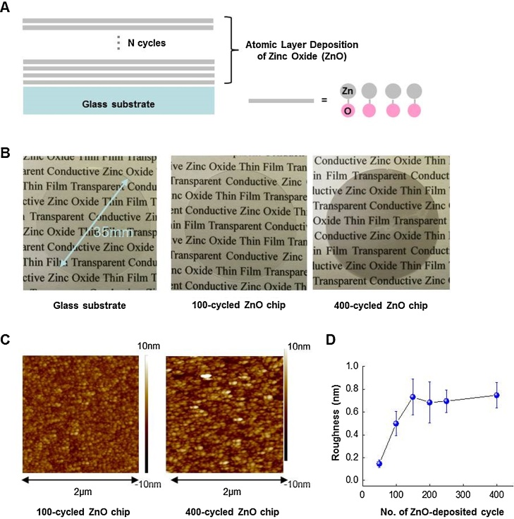
Fig. 1.
Growth of ZnO thin films and its characteristics. (A) A schematic depiction of ALD-processed ZnO thin film with different thickness. (B) A 6-well plate-sized glass substrate was used to prepare chips deposited by ZnO thin films. The transparent 100-cycle and 400-cycle ZnO chips are shown. Also shown are topological images (C) and a plot of surface roughness (D), analyzed by AFM, versus the number of ALD cycles, respectively.

