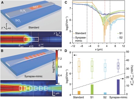
Fig. 2. Finite element method (FEM) simulations of the photonic synapse with different structures.

(A) Top: Schematic shows photonic synapse with a standard design: a straight waveguide with a thin film of GST (6 μm × 0.8 μm, orange block) on top. Bottom: TE mode E-field distribution at the surface of the waveguide with the entire GST film (white box) in the crystalline state. (B) Top: Schematic shows photonic synapse with synapse-mimic design: a tapered waveguide with six discrete GST islands (1 μm × 0.8 μm each) on top, which is the structure used in our experiments. Bottom: E-field distribution with all GST islands in crystalline states. (C) E-field distributions along the center line of the waveguide surface. The yellow, purple, green, and cyan curves correspond to the E-field distribution along the dashed horizontal lines in (A) and (B) (standard and synapse-mimic) and fig. S3 (A and B) (S1 and S2), respectively. The dashed red (black) lines illustrate the left and right boundaries of the GST film (discrete GST islands) in standard and S1 (synapse-mimic and S2) designs. (D) Top: Statistical results of the E-field inside the GST film or islands (square, average value; box, SD; bottom and top lines, minimum and maximum values). Bottom: The ratio between the average E-field at the output () and input () edges of the GST film or islands corresponding to the orange dashed lines in (A) and (B) and fig. S3 (A and B).
