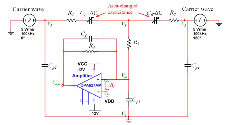
Figure 2.
Model of the transducer including parasitic capacitance, where C0+ΔC and C0-ΔC are the differential area-changed capacitances, Cp1 and Cp2 are the parasitic capacitances of the electrodes on the top die, Cp3 is the parasitic capacitance between the electrodes on the proof mass and silicon substrate, and R1, R2 and R3 are the resistances of the deposited wires for signal transmission, Cf and R4 are the electron devices of the amplifier circuit. The silicon substrate connects to the ground through ohmic contact to overcome influences of Cp1 and Cp2 on the sensitivity and offset.

