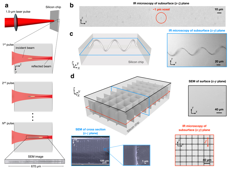
Figure 1. Creation of 3D index modification inside silicon.
(a) The schematic shows laser pulses incident on a Si chip. The pulse collapses and modifies local Si crystal structure, which constitutes a building block for more complex structures. Consecutive laser pulses focus to shifted positions, axially elongating the structured region. The inset shows a scanning electron microscope (SEM) image of a rod-like structure in Si. (b) IR image of an array of 1 µm-sized voxels each created by a single laser pulse. (c) IR image of a 1 µm-thick, 1 mm-long helix exemplifies point-by-point fabrication of an in-chip 3D structure. (d) Various 3D structures can alternatively be formed using rod-like structures as building blocks. These 1-µm wide structures can range from 20 µm to hundreds of micrometres along the laser propagation direction (z-axis). SEM (for top surface and cross-section) and infrared (IR) transmission microscope (for subsurface) images correspond to colour-labelled planar sections of the 3D schematic. The subsurface mesh is directly revealed in the IR image, whereas the top (shown) and bottom (not shown) surfaces remain unscathed.

