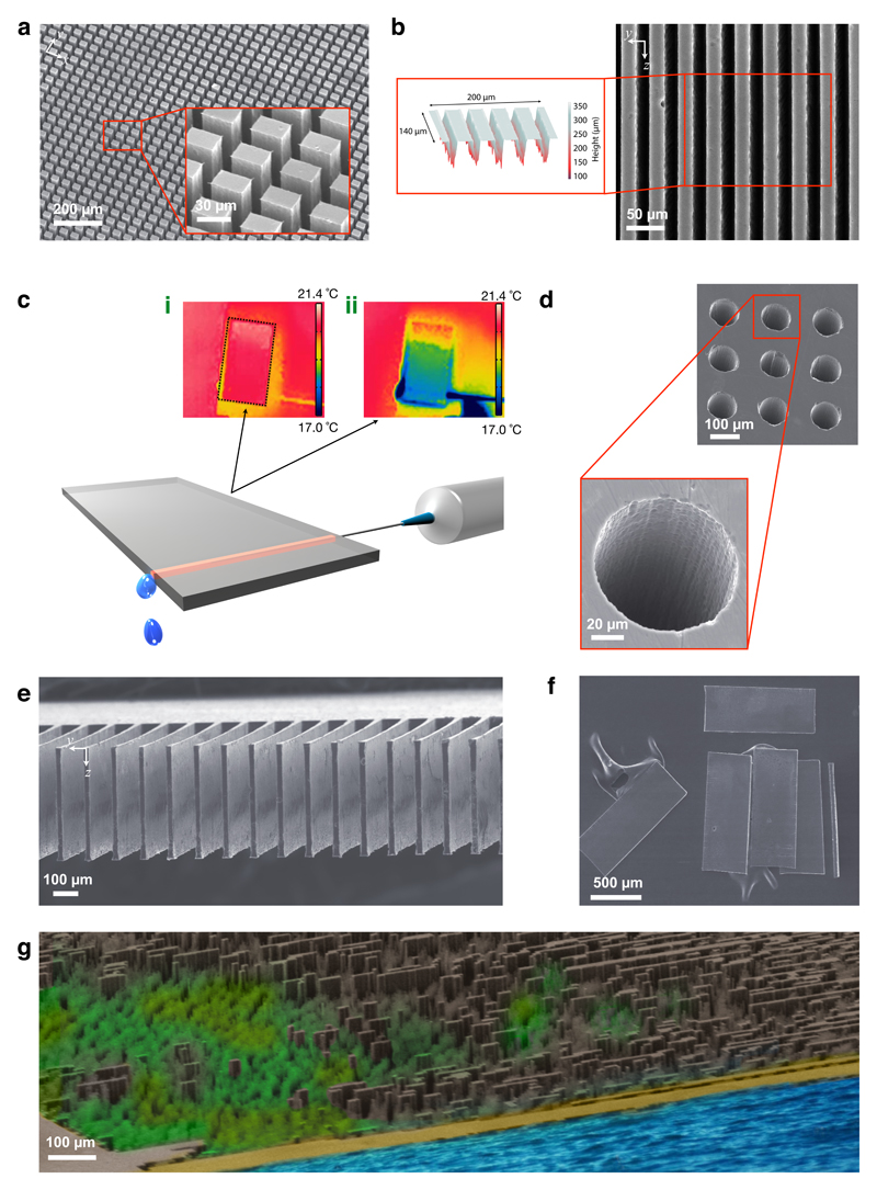
Figure 4. Sculpting of 3D arbitrary micro-architectures.
(a) SEM image of large-area covering, high-aspect-ratio micropillars revealed after chemical etching. The inset shows a close-up view of the etched micropillar array. The pillars have 20 × 30 µm top surfaces, and their heights extend ~500 µm along the laser propagation direction. (b) SEM image of a sidewall of a Si chip, showing embedded microchannels. Inset shows laser scanning microscopy of the channels, which penetrate hundreds of micrometres into the chip. (c) The illustration shows an 8 mm-long microfluidic channel carrying cooling water into a chip. Thermal camera images (i) before and (ii) after passing the water shows that the surface temperature of the chip decreases by 4°C within a few seconds. (d) SEM image of entrance of through-Si vias that cut across the entire chip. (e) SEM image of 3D cantilever-like structures. (f) SEM image of controlled slicing of a chip into ~30 µm-thick plates. (g) An artificially coloured view of a micro-cityscape created out of silicon.

