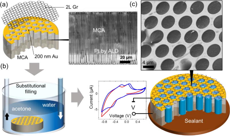
Figure 1.
The fabrication and filling of the MCA matrix with an analyte. (a) A 200 nm/10 nm Au/Cr film was sputtered sequentially onto the front side of the MCA silica matrix for metallization and reliable adhesion of graphene. For electrochemical measurements, the interior of the MCA channels was coated with 40 nm of Pt as a counter-electrode using atomic layer deposition (ALD). Bilayer graphene was transferred onto the front side of the MCA using PMMA as a sacrificial layer. The inset shows a cross-sectional SEM image of the MCA half-coated with Pt. (b) PMMA was dissolved in an acetone bath followed by a gradual substitution with isopropyl alcohol (IPA) and water. (c) Depending on application, the sample was sealed either with ultraviolet (UV) curable adhesive or liquid metal (galinstan). The inset demonstrates the SEM image (3 keV) of water filled MCA channels. Experimental voltammograms recorded in a 1 mol/L CuSO4 solution are shown here to demonstrate the electrochemical capabilities of the MCA platform.

