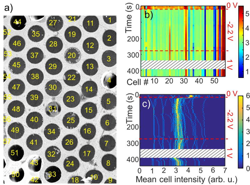
Figure 6.
Copper electroplating and stripping: multichannel FOV. (a) an SEM image of a 48 µm × 34 µm area of an MCA filled with 1 mol/L CuSO4 electrolyte with 57 randomly selected cells. The image is a captured frame from a video file that recorded copper deposition and stripping process. It presents a moment at time t= 206 s, when a negative bias of 2.2 V was applied to the top (graphene) electrode and copper deposition took place. Cell # 20 shows large grown copper crystals. The image was used for high throughput analysis. (b) Color diagram of the mean SEM signal intensity within each of the 57 cells shown in (a) as a function time and cell number. Color bar is in arbitrary units of mean SEM intensity. Bias applied to graphene was changed in steps over time and is shown on the right of the diagram by dashed lines. Note how intensity of cell 20 changes as copper is plated at negative and stripped at positive potential. (c) Color-coded histogram representing distribution of mean SEM signal intensity within 57 cells plotted vs. time. Colorbar shows number of cells with a given mean intensity. The maximum of the histogram changes only slightly, as Cu deposition in most cells was limited, however several cells show strong increase of the signal during deposition (lines of the histogram that migrate to the right). The white patterned strip between 350 s and 400 s in panels (b) and (c) is a gap in data due to video recording freeze during the experiment.

