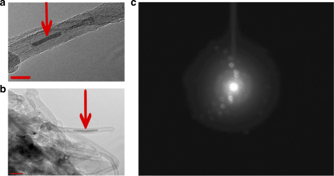
Fig. 4.
High resolution TEM images. Panels a, b show a solid structure on the short multiwall carbon nanotubes (indicated by arrows) obtained at −165oC. The scale marker (bottom left) in panel a is 10 nm and the scale marker (bottom left) in panel b is 20 nm. The selected area electron diffraction pattern is shown in panel c. The inner ring is from the carbon nanotubes and the second ring is from the synthesized phase which is highly crystalline. Analysis of the electron diffraction pattern using FFT (Fast Fourier Transform) is displayed in Supplementary Fig. 3 from selected regions of the image in panel a

