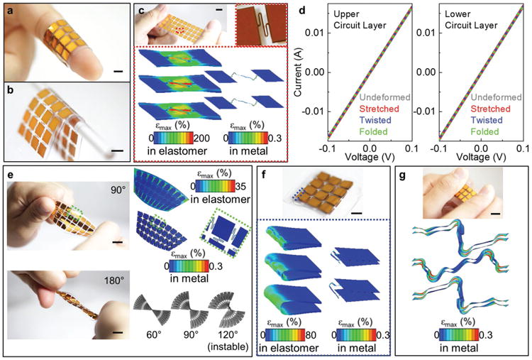
Figure 6.

Mechanics and performance of a representative, structurally optimized electronic module with bilayer circuit construct. a,b) Optical images of the device compliantly wrapped around (a) an index finger and (b) a stirring rod. (Scale bar: 500 μm). c) Optical image and FEA results of the device in a uniaxially stretched configuration. (Scale bar: 1 cm). In FEA model, the unit cell (magnified in the optical image) is elongated by 42%. Left column: deformed composite superstrate (top), inter layer (middle), and composite substrate (bottom). Right column: deformed upper (top) and lower (bottom) circuit layer. d) Current–voltage curves measured from the serpentine interconnects under different deformations (undeformed, stretched, twisted, folded). e) Optical images and FEA results of the device in a twisted configuration. In experiment, the device was twisted by 90° (top left) and 180° (bottom left). Structural instability was observed at 180° twisting. (Scale bar: 1 mm.) FEA results show the global deformation of elastomer (1st row) and circuit layers (2nd row, left), and highlight the local site with most severe deformation (2nd row, right). FEA images in the 3rd row show the side view of the circuits before (60° and 90°) and after (120°) the onset of structural instability. f) Optical image and FEA results of the device in a temporarily folded configuration. (Scale bar: 500 μm). FEA models the local site with most significant deformation. Left column: deformed composite superstrate (top), interlayer (middle), and composite substrate (bottom). Right column: deformed upper (top) and lower (bottom) circuit layer. g) Optical image and FEA results for stretching a folded device. (Scale bar: 1 mm). FEA results show a set of deformed serpentine interconnects in the device (elongated by 23%) in a worst-case scenario. Top: upper and lower circuits in the 1st device layer. Medium: lower and upper circuits in the 2nd device layer. Bottom: upper and lower circuits in the 3rd device layer. In all FEA results, color denotes maximum principal strain in metal or in elastomer.
