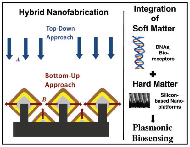
Figure 1.
Schematic illustrating the development of novel, plasmonically active, diamond-shaped nanowire structures employing a hybrid approach combining the top-down methodologies A (deep-UV lithography, dry etching, and metal evaporation) with bottom-up methodologies (epitaxial silicon–germanium growth, including lateral diamond-shaped silicon–germanium nanowire growth B that bridges the gaps between the nanowires and the development of triangular nanostructures between the diamond-shaped nanostructures, as well as atomic layer deposition), such that chips containing these nanowire structures could be employed for plasmonics-based sensing of chemical and biological molecules.

