Figure 2.
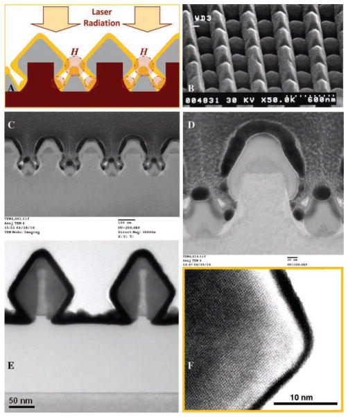
A) Schematic of Si1−xGex nanowires (light grey color) with a diamond-shaped structure, epitaxially grown from silicon nanowires (magenta color). The Si1−xGex nanowires were coated with gold film (yellow color). When laser radiation is incident on the gold-coated DNWs, SERS hotspots H are produced between the diamond-shaped and the triangular nanowire structures. B) Scanning electron microscopy (SEM) image of 2D gold-coated Si1−xGex nanowires. C, D) TEM cross-section image showing small triangular sections formed in between the diamond NWs. E) TEM cross-section image showing ALD of platinum (black color) on the diamond-shaped Si1−xGex nanowires (dark grey color) formed on SOI wafers. F) High-resolution TEM image of the Si1−xGex nanowires.

