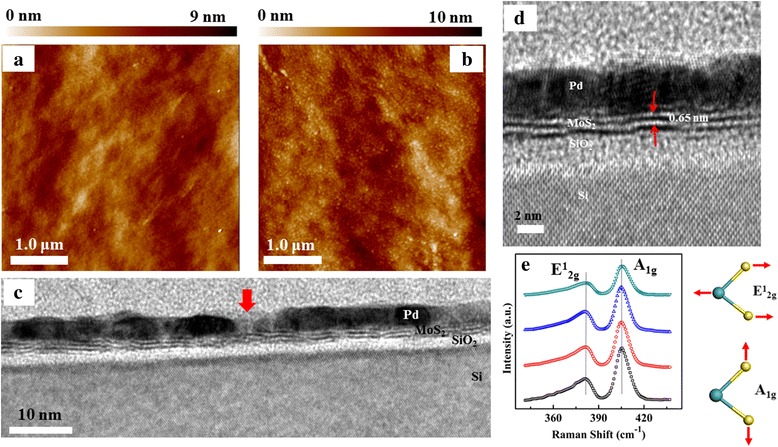
Fig. 2.

AFM images of the MoS2 layers a without Pd decoration, and b with 5-nm Pd decoration. c HRTEM image of the Pd-decorated MoS2 layers on the Si substrate. The red arrow denotes the gap between two Pd nanoparticles. d Enlarged HRTEM image. e Typical Raman spectra of the as-grown MoS2 layers on Si from different regions of the sample
