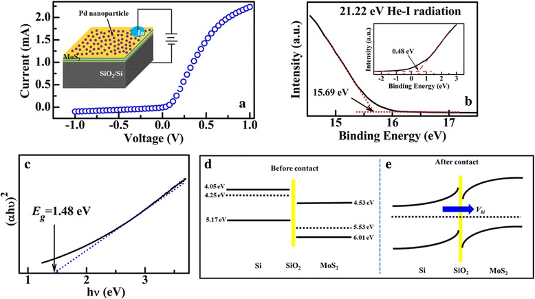
Fig. 4.

a I-V characteristics of Pd-decorated MoS2/Si heterojunction. The inset shows the schematic illustration for the measurements. b UPS spectra of the MoS2 layers on Si substrate. c Curve of (αhν)2 vs hν of the MoS2 layers. The energy band diagram at the MoS2/Si interface before contact (d) and after contact (e)
