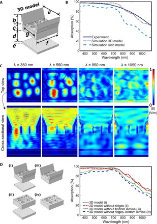
Fig. 2. 3D FEM optical simulations of the micro- and nanostructures of the P. aristolochiae butterfly.

(A) 3D model of the butterfly scale and corresponding parameters extracted from SEM images. The dimensions of this model are as follows: a = 2.0 μm, b = 1.2 μm, c = 0.8 μm, d = 1.2 μm, e = 0.22 μm, f = 5.0 μm, and g = 1.5 μm. (B) Comparison of experimental and simulated absorption spectra under normal incidence. The experimental data are measured with an integrating sphere in the matt black region (solid line). The dashed line corresponds to the simulated 3D model with an air-filling fraction of 59%. For comparison, we also constructed an unpatterned slab model by squeezing the 3D original model into a slab with the same bottom area and volume (long dashed line). (C) Normalized electric field intensity distribution calculated for normal incidence and wavelengths of 350, 550, 850, and 1050 nm. (D) Influence of different structural components of the scale architecture of P. aristolochiae on the absorption properties. The schematics represent different 3D models. The corresponding simulated absorption spectra are shown in the plot on the right. The nanohole array is found to be the primary contributing element for the absorption in the UV-vis–NIR region.
