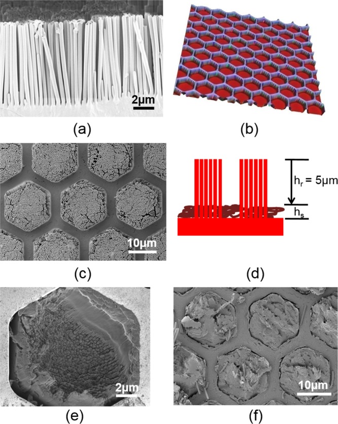
Figure 3.

PS nanopillar arrays. (a) Scanning electron microscopy (SEM) image of the cross section of the PS nanopillar array. (b) Confocal microscopy image of the pattern on the nickel mold insert. (c) SEM image of patterned PS nanopillar array. (d) Schematic drawing shows that the remaining height (hr) of PS nanopillars (red) is designed to be 5 μm. SEM image of (e) footless nanopillars retained in the nickel stamp after shearing and (f) corresponding supporting layer.
