Figure 3.

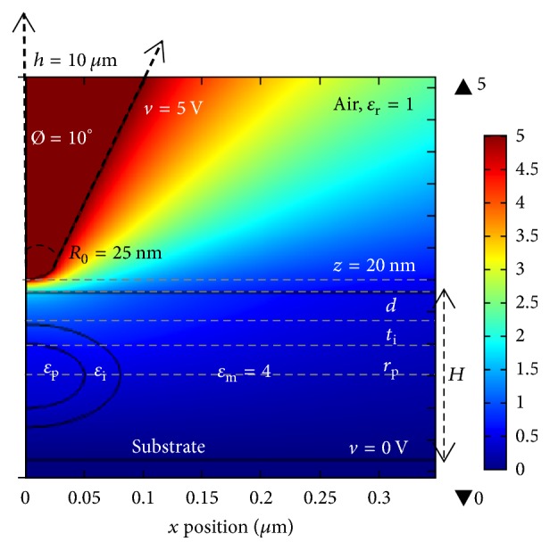
Electric potential map in volts obtained with a 2D axisymmetric model of the EFM tip, nanodielectric sample, and substrate.

Electric potential map in volts obtained with a 2D axisymmetric model of the EFM tip, nanodielectric sample, and substrate.