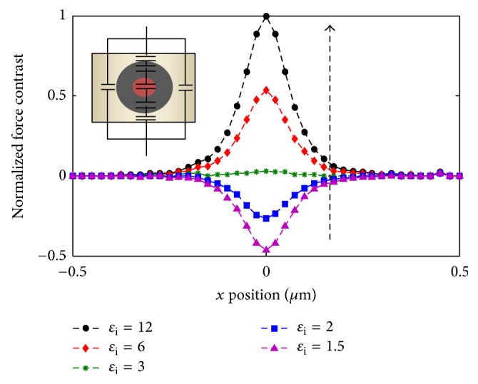
Figure 4.

EFM normalized force contrast on a 1 μm scan over a nanodielectric of εm = 4, εp = 10, rp = 25 nm, and ti = 20 nm and at 15 nm from upper and lower surfaces; inset: capacitance model of the nanodielectric comparing center to border scan line regions.
