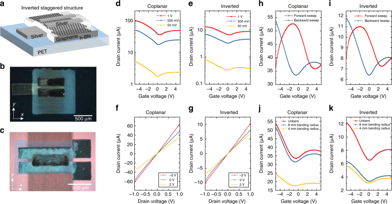
Fig. 3.
Inkjet-printed inverted-staggered FET on PET. a Schematic of a printed inverted-staggered FET heterostructure. Optical microscopy images (dark field) of the b inverted-staggered and c coplanar FET heterostructures on PET with channel lengths of 50 and 65 μm, respectively. d, e Transfer characteristics and f, g linear output characteristics of the FETs as a function of V ds. h, i Transfer characteristics of the FETs with observable hysteresis depending on sweep direction at V ds = 1 V. j, k Transfer characteristics of the FETs as a function of bending radius in the x-direction at V ds = 1 V

