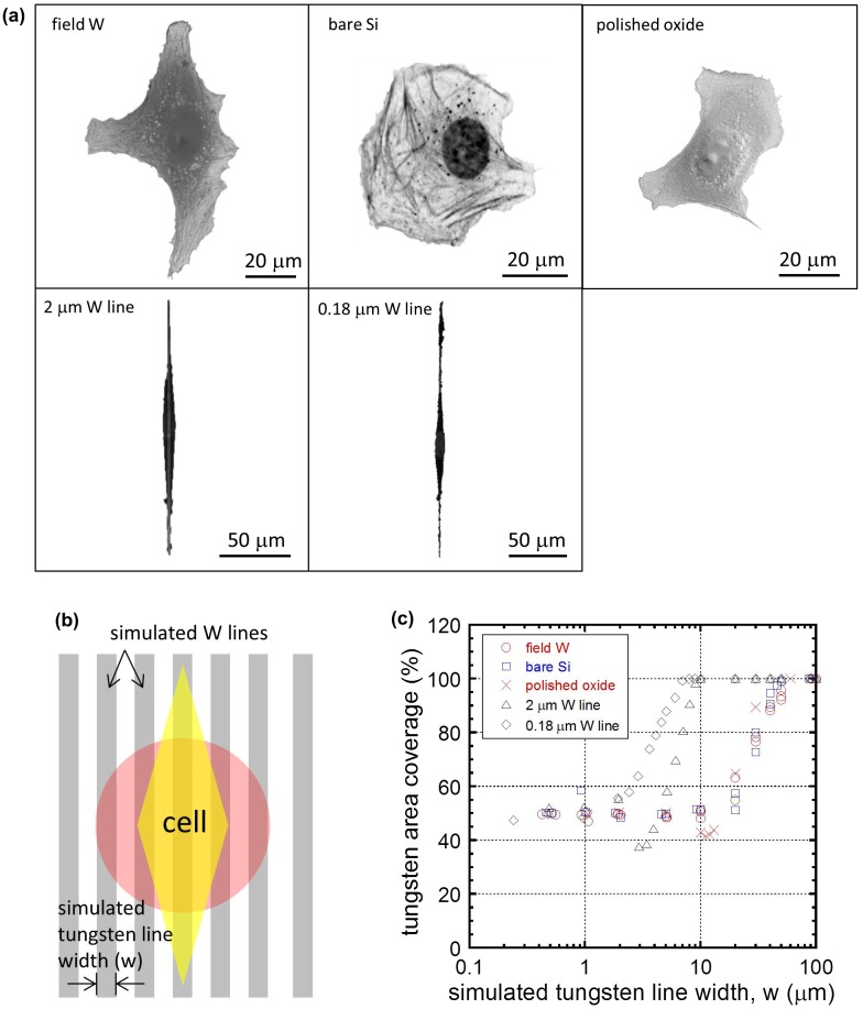
Figure 11.
(a) Observed cell morphologies on different surfaces (polished field tungsten area – field W; bare silicon – bare Si; polished silicon oxide – polish oxide; surface with isolated 2 μm line – 2 μm W line; surface with 0.18 μm tungsten isolated line – 0.18 μm W line) with a superimposed simulated comb pattern used in the calculation of coverage in (c). (b) Schematic drawing indicating cell orientation relative to the simulated comb structure; the pink circle and yellow diamond represent cells with random and elongated shapes, respectively. (c) Cell-tungsten coverage of cells plotted as a function of simulated tungsten line widths (w).

