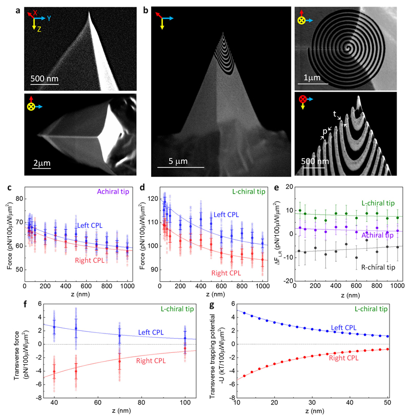
Figure 3. Enantioselective optical forces with achiral and chiral tips.
a, SEM images of an achiral silicon tip. b, SEM images of a chiral tip, which is made with focused ion milling (see Methods). “t” denotes thickness of the gold coating; “p” is the period of the spiral. c, Measured optical forces using the achiral tip with left-handed (blue) and right-handed (red) CPL, at 750 nm. d, Measured optical force using the chiral tip with left-handed CPL (blue), and right-handed CPL (red). e, Comparison of the enantio-selectivity in the measured force (difference in the forces with left- and right-handed illumination), with both achiral and chiral tips. f, Measured transverse forces with the chiral tip, with left-handed (blue) and right-handed (red) CPL illumination. In all panels, the void dots are raw data, the solid dots are mean values, and error bars show standard deviations. The solid curves in panels (c), (d), and (f) are fitted with exponential decay equations, while solid curves in panel (e) are fitted with polynomial equations. g, Simulated transverse trapping potentials exerted from the coaxial aperture on a chiral nanoparticle with size comparable to the AFM tip radius. Note that we plot the negative of the trapping potential to emphasize the similar trend as the measurements.

