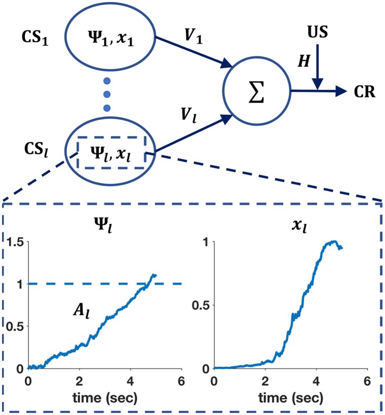
Fig 1. Connectionist diagram of RWDDM.
Each CS unit is connected to a summing junction (labelled Σ) via a modifiable link V. The output of the summing junction is the CR. The US is represented as a teaching signal with a fixed weight H. Each CS unit has its own timer Ψ and representation x. The bottom panel shows a zoomed-in view of the timer Ψl and CS representation xl associated with CSl. The timer slope Al is tuned to a 5-second CS duration.

