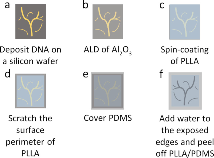
Figure 1.
Fabrication process of a polymer stamp using a DNA nanostructure master template with a protective Al2O3 film. (a) DNA nanostructures are deposited on a silicon wafer. (b) The silicon wafer is coated with Al2O3 by atomic layer deposition. (c) A polymer film (e.g., PLLA) is spin-coated onto the silicon wafer. (d) The edges of the polymer film is scraped off with a blade. (e) A PDMS film is adhered to the polymer film as a backing support. (f) Droplets of water are added to the exposed edges of the silicon wafer and the PLLA/PDMS film is peeled off.

