Figure 3.
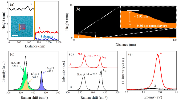
(a) AFM height profile of laser irradiated region (A), non-irradiated region (B), and substrate (ground): the measured thickness between A and B is ~2.88 nm; between the substrate and A is ~0.9 nm (Inset shows the optical image of the laser irradiated area for 15 seconds on 5 × 5 μm, scale bar: 5 μm). (b) An average AFM height profile of the laser irradiated region (A) shows the etched thickness of ~2.92 nm. (c) Raman spectrum of a single-layer WS2 film (A) using the 514 nm laser excitation and its Lorentzian peak fits. (d) Raman spectra showing the peak distance (△k) between 2LA and A1g measuring at 65.5 cm−1 and 70.5 cm−1 for regions A and B, respectively. (e) PL spectra of region A and B showing ~6 times increase of PL emission intensity and ~0.05 eV shift of PL peak position by the laser irradiation.

