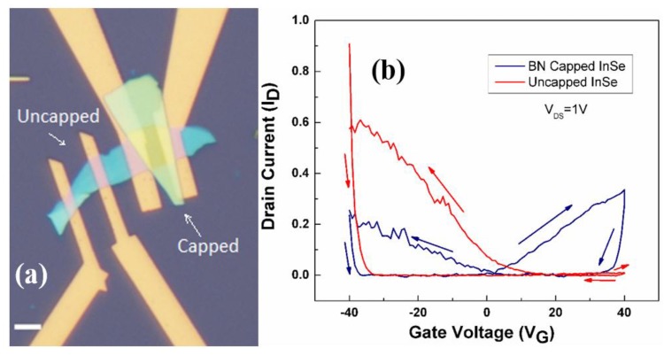
Figure 7.
(a) Optical image of typical InSe back-gate transistor devices: in one device the channel is capped with a flake of hexagonal boron nitride (h-BN), whereas the other channel is exposed to atmosphere. (b) Behavior of the drain current as a function of the gate voltage for the cases of capped and uncapped InSe-based transistors. The uncapped device shows dominant p-type transport (even if with notable hysteresis), while the capped device noticeably displays ambipolar transport. Reproduced with permission from Ref. [20]. Copyright Royal Society of Chemistry, 2016.

