Fig. 1.
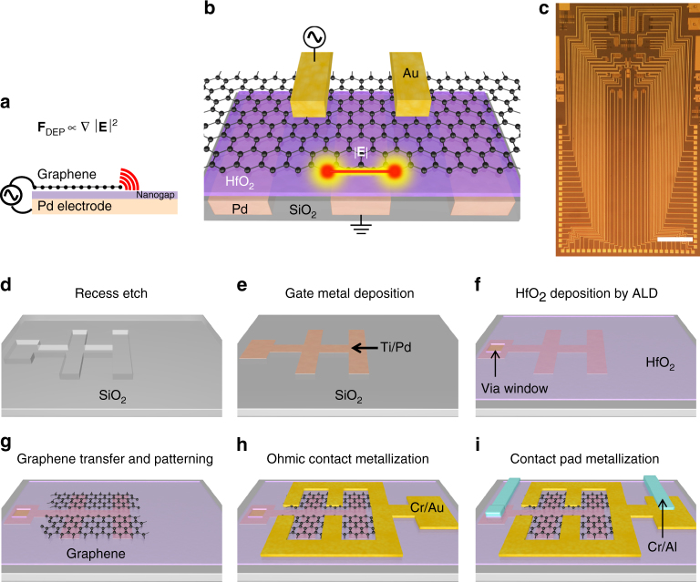
Graphene as an electrode for dielectrophoresis. a Being a gradient-dependent phenomenon, DEP force is increased as the radius of curvature of an electrode is reduced. The edge of graphene could provide the smallest possible radius of curvature. b An illustration showing the region of strongest electric field gradient is generated at the intersection of the edge of the graphene by applying an AC bias between the graphene contact electrode (gold) and palladium gate electrode. c A photograph of the chip. Scale bar: 2 mm. d The gate electrode patterns were created on SiO2 substrate by combining photolithography with reactive ion etching and wet etching. e Ti/Pd layer was deposited followed by lift off to create the gate electrodes. f 8-nm-thick HfO2 was deposited to coat the entire surface with an insulator. A via window was created for contact pad metallization with the Pd gate electrode at a later step. g Single-layer graphene grown by chemical vapor deposition process was transferred to the dielectric layer by a wet transfer process, followed by patterning using photolithography and O2 plasma etching. h Ohmic contacts were made by photolithography, Cr/Au deposition by electron-beam evaporation and lift off. i A thick metal layer of Cr/Al was added to create low-resistance electrical leads for electrical probing

