Fig. 2.
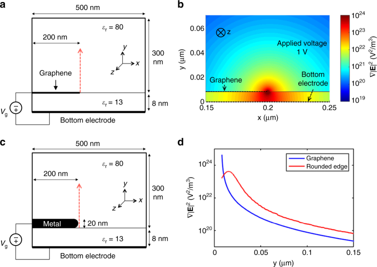
Self-consistent calculations of field gradients around a graphene edge. a Graphene electrode of zero thickness is placed 8 nm away from the bottom electrode and gradient of electric field intensity is calculated when a bias is applied between the electrodes. b Intensity plot in logarithmic scale of computed at the back gate voltage V g = 1 V (the flat band voltage is set to zero) showing a strong peak at the graphene edge. An 8-nm-thick HfO2 layer with a dielectric constant of 13 was assumed between the electrodes. The rest of the simulation domain was assumed to be water with a dielectric constant of 80. c Vertical cut-line (noted by red arrow) of the intensity plot in a at x = 0.2 μm (position of the graphene edge), compared with the result of a similar simulation where graphene is replaced by a metal with a thickness of 20 nm and a realistic round edge with radius of curvature 10 nm. d The two profiles are similar but the magnitude of at the edge position is greatly enhanced in the graphene case because of its one-atom thickness

