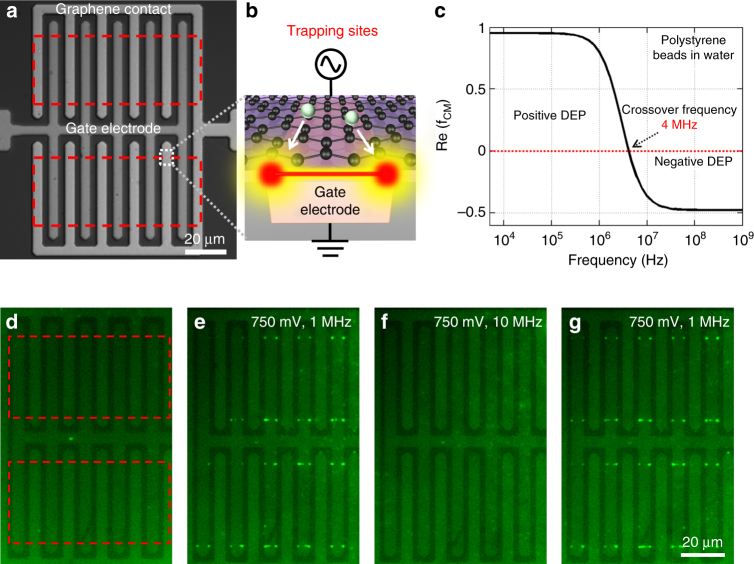
Fig. 3.
DEP manipulation of 190 nm polystyrene beads using graphene electrode. a A bright field microscopic image of the electrode design is shown with the location of the graphene patterns marked with red rectangles. b Applying an AC bias between graphene contact and the bottom gate electrode creates strong field gradients at the graphene edge. However, the region of strongest field strength resides at the intersection points of the graphene edge and the bottom electrode edge (red circles)—“trapping sites”. c Clausius-Mossotti (CM) factor plot for polystyrene beads in water with a conductivity of 4 μS/cm. d A green background was observed before applying voltage from the bulk solution. e−g 190 nm polystyrene beads were trapped e at the trapping sites due to positive DEP (750 mV, 1 MHz). The beads can also be released f due to negative DEP (750 mV, 10 MHz) and then retrapped again g by applying positive DEP

