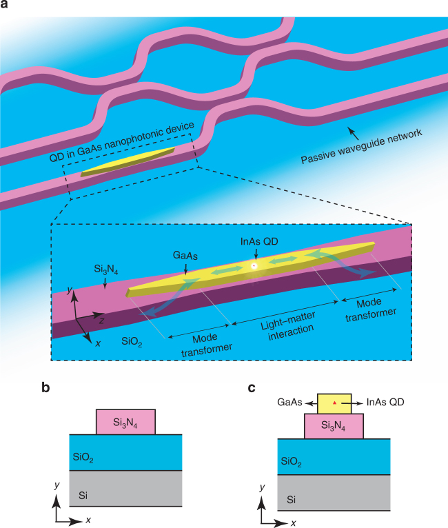
Fig. 1.
Principle of operation and device geometry. a Conceptual quantum photonic circuit composed of a passive waveguide network with a directly integrated GaAs nanophotonic device (exemplified by a nanowaveguide) containing a single quantum dot. A zoomed-in image of the GaAs device region (inside the dashed boundary box) shows details of the geometry and operation principle of the hybrid photonic integration platform. The light–matter interaction section of the device promotes efficient coupling between a confined electromagnetic field (in this case, a wave confined in a GaAs nanowaveguide) and a single-InAs QD embedded in the GaAs. Adiabatic mode transformers allow light from the QD in the light–matter interaction region to be efficiently transferred to a Si3N4 waveguide, and, conversely, also allow the QD to be accessed efficiently with resonant light guided by the Si3N4 waveguide. b, c Cross-sections of passive Si3N4 and active GaAs waveguides that form the core elements of the integration platform

