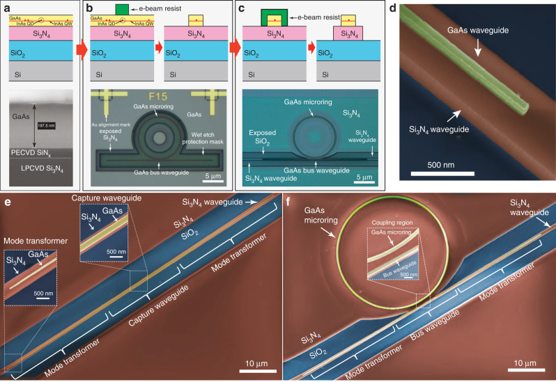
Fig. 3.
Device fabrication. a Top: schematic of the bonded wafer stack used in fabrication, consisting of a top III–V layer, containing InAs QDs, that is directly bonded on top of a Si/3 μm SiO2/550 nm Si3N4 stack. Bottom: cross-sectional scanning electron microgaph (SEM) of bonded wafer stack. The ≈30 nm SiNx layer was grown on the GaAs wafer surface prior to bonding. b Top: GaAs device lithography and etching steps. Bottom: optical micrograph of etched GaAs microring resonator and bus waveguide. Au aligment marks used for registered electron-beam lithography are visible. A wet etch protection resist mask (not depicted in the schematic—Supplementary Note 2) is also visible. c Top: Si3N4 waveguide lithography (aligned to the previously etched GaAs device) and etching steps. Bottom: optical micrograph of GaAs microring resonator and bus waveguide, and underlying Si3N4 waveguide. d False-color SEM of tip of mode-transformer geometry, common to both devices in (e, f). e False-color SEM of fabricated GaAs waveguide (yellow) on top of Si3N4 (red) waveguide. Blue regions are exposed SiO2. Insets show details of the mode transformer end tip and the QD photon capture waveguide. f False-color SEM of GaAs microring and bus waveguide, and underlying Si3N4 waveguide. Inset shows details of the microring-bus waveguide evanescent coupling region

