Figure 3.
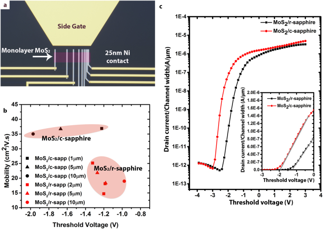
FET device comparison for monolayer MoS2/r-sapphire and MoS2/c-sapphire. (a) 100× optical microscopy (OM) image of a TLM device, which consists of back-back FETs of varying channel length. Note that the MoS2 channel is false-colored for easier visualization. The side-gate structure at the top of the image is used to make contact with the gate probe in order to ensure constant side-gate-MoS2 distance and consistent, efficient ion response across multiple devices and device structures. (b) A plot of field-effect mobility vs threshold voltage for the devices on the two different sapphire surfaces. MoS2/r-sapphire devices are clearly p-doped relative to MoS2/c-sapphire and also suffer from slightly lower mobility which is attributed to increased carrier scattering from O-defects in the film as a result of the r-plane surface termination. (c) Comparison of transfer curves between identical MoS2/r-sapphire and MoS2/c-sapphire devices, further demonstrating the threshold voltage shift for the different surface terminations as well as the high on/off ratio and steep turn-on for both cases. In this instance, Lch = 10 µm, drain current is normalized by channel width, and Vd = 500 mV. The inset of (c) is a magnified plot of the same curves in linear scale to better visualize the actual threshold voltage positions and difference in transconductance (gm) represented by the slope.

