Fig. 6.
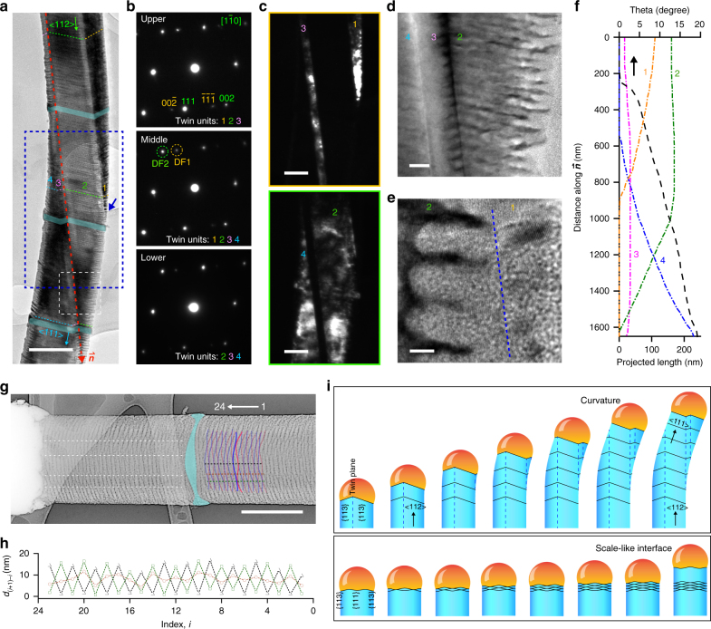
Atomic gold patterns enable the discovery of new crystal growth behaviors. a A BF TEM image of the nanowire with multiple twin units labeled by numbers. The growth orientation is shifted gradually from <112> to <111>. Cyan ribbons highlight the intrinsic segments. Scale bar, 200 nm. b SAED patterns taken at upper, middle, and lower portions of the nanowire in a. c DF TEM images formed by selecting diffraction spots marked by yellow (DF1) and green (DF2) dashed circles in b. Scale bars, 100 nm. d, e HRTEM images from different regions in a, marked by a white dashed box (d) and a blue arrow (e). Scale bars, 20 nm (d), 5 nm (e). f Growth behavior analysis shows a smooth transition of the nanowire orientation from a <112> (marked by in a) to a <111> direction. Projected lengths of individual twin units and the nanowire angular orientation are plotted along . g A TEM image (with color inversion) of a nanowire with a scale-like TPB. Scale bar, 200 nm. h The growth behavior is analyzed by tracking spacing d (i+1)–i between adjacent wavy lines (blue and pink lines) at three different locations (black, brown, and green dashed lines in g). The white arrow in g indicates the direction of analysis. i Schematics of the growth dynamics. A curved nanowire can be formed when it gradually switches the growth orientation from <112> to <111> (black arrows), without involving a kink unit. During the transition, the droplet crosses multiple twin boundaries, marked by black dashed lines. A scale-like alloy/Si interface is formed when the TPB oscillates between two wavy line shapes. The cyan ribbon in a and g marks an intrinsic segment

