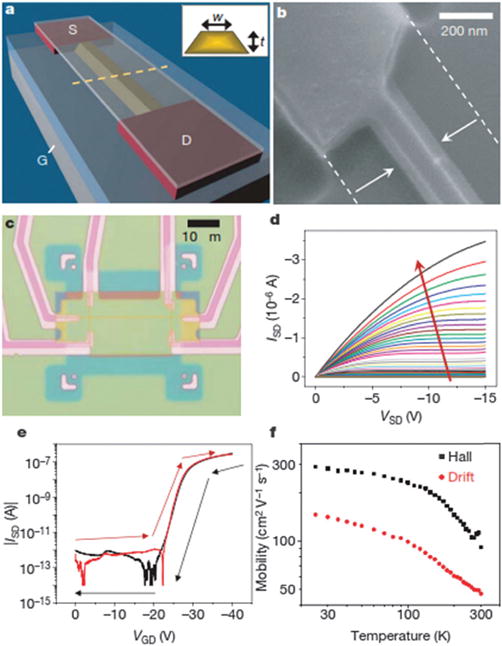
Fig. 10.

Device fabrication and electrical performance. (a) Schematic after anisotropic etch. The silicon-on-insulator active channel (yellow, width w and thickness t) is undercut etched, whereas degenerate leads (red) are etch resistant. The source (S), drain (D), and underlying back gate (G) are labelled. (b, c) Scanning electron micrograph (b) and optical micrograph (c) of a completed device. (d) ISD (VSD) (w = 50 nm, t = 25 nm) for varying VGS (0 to −40 V, ΔV = −1 V), illustrating p-type accumulation mode behaviour. (e) |ISD|(VGD) for VSD = 1 V for forward (red) and reverse (black) sweep. (f) Accumulation-mode Hall and drift mobilities versus temperature (w = 300 nm, t = 25 nm). Copyright Nature, Nature Publication Group.131
