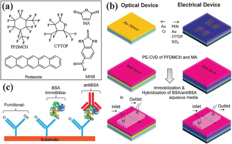
Fig. 17.

Schematic representation of a bottom-contact pentacene OTFT and optical sensors. (a) Chemical structure of the organic molecules. (b) (Right, top to bottom) fabrication procedure for a bottom-contact OTFT with CYTOP (15 nm)/SiO2 (200 nm) dielectric layer, source–drain electrodes with a W/L of 10 and a 30 nm pentacene layer followed by the top PE-CVD protective and functional layer. (Left, top to bottom) Fabrication procedure for the optical device with Au (50 nm)/Cr (2 nm)/LaSFN9 glass followed by the top identical PE-CVD protective and functional layer. (c) Schematics of the surface modification to immobilize the BSA for selective antiBSA detection. Copyright Journal of the American Chemical Society, American Chemical Society.139
