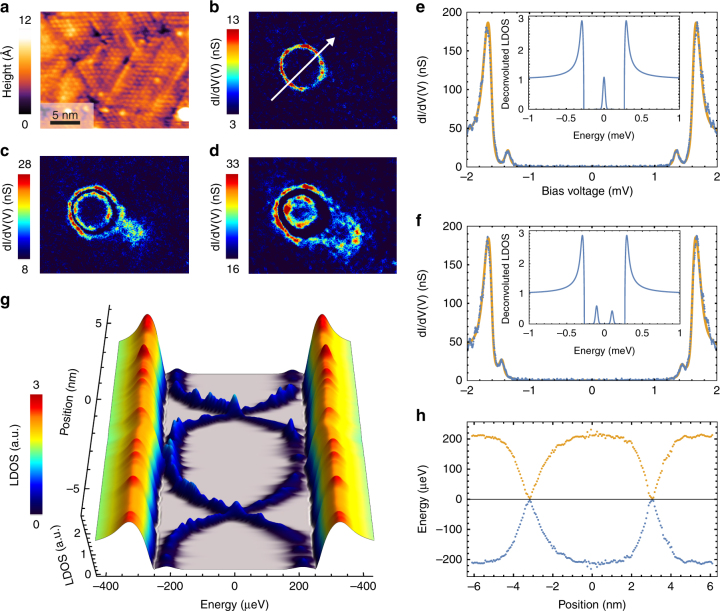
Fig. 2.
Topological edge states. a Topography of an area 23 × 18 nm2 measured by scanning tunneling microscopy (bias voltage −50 mV, tunnel current 30 pA). b–d Scanning tunneling spectroscopy dI/dV(V) conductance maps of the same area at three different voltage biases (1.30 meV, 1.43 meV, 1.5 meV, respectively) showing the energy evolution of the edge states appearing at the frontier between a topological and a trivial superconductor. This area corresponds to the same region of the sample as the one shown on image a. e The blue dotted curve shows a dI/dV(V) conductance spectrum measured at the intersection between the cut and the ring shown in b. The conductance spectra are a convolution of the sample LDOS with the BCS gap of the Pb superconducting tip. The orange curve is a fit of this convoluted LDOS. The corresponding deconvoluted LDOS is shown in the inset. It exhibits a pic at the Fermi level. f The same as e but for a spectrum measured in the upper part of the outer ring shown in image c. The deconvoluted LDOS shown in the inset displays two in-gap peaks at symmetric energies. g Line-cut of the deconvoluted LDOS along the dotted line in b showing the spatial dispersion of the topological edge states. The edge states displays a X-shape at the interface of the cluster. h Energy position of the in-gap states extracted from the fit of the linecut shown in g, no anti-crossing is observed

