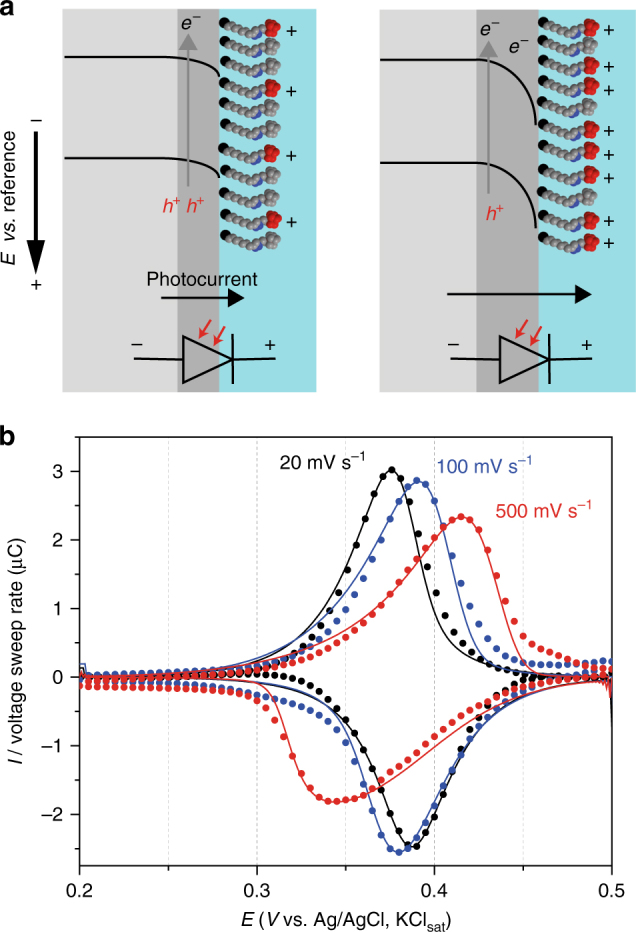
Fig. 5.

Validation of the model and its implications for the correct kinetic analysis of charge-transfer reactions at semiconductors. a Energy-level diagram depicting the distortion of the semiconductor side of the barrier for a-Si photocathodes due to electrochemically induced changes to surface charges. b Experimental (symbols) and simulated voltammograms (solid lines, model 3, Supplementary Note 6) for S-2 samples over a wide range of voltage sweep rates (20–500 mV s−1). Simulation parameters are listed in Table 1
