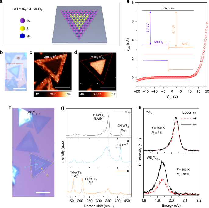
Fig. 6.
Formation of MoS2/MoTe2 lateral junction and WS2−xTex alloy. a Schematic of 2H-MoS2/2H-MoTe2 in-plane heterojunction. b–e Optical micrograph (b); scale bar, 20 μm, confocal Raman mapping of E1 2g 2H-MoTe2 (c), and 2H-MoS2 (d) for MoTe2/MoS2 junction; scale bars, 50 μm and the corresponding diode I–V curve (e). A clear diode behavior with the band diagram of the MoTe2/MoS2 heterostructure reveals a type-II junction. For electrical measurements, source (MoTe2) and drain (MoS2) electrodes were fabricated by depositing 5/50 nm Cr/Au. f Optical micrograph of tellurized monolayer WS2 flakes. WTe2/WS2−xTex junction; scale bar, 20 μm. g Raman spectra from each region of a and b in f. The Raman spectrum of 2H-WS2 is also provided for comparison. h Circularly polarized PL spectra of 2H-WS2 and the WS2−xTex alloy (at 300 K) excited by σ+ polarized light at energy of 2.33 eV. The PL is red-shifted to ~ 0.1 eV and valley polarization is enhanced up to 37% in the WS2−xTex alloy. Valley polarization (P c) is defined as

