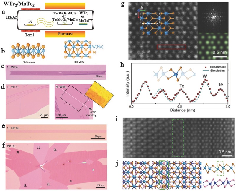
Figure 4.

a) Illustration of WTe2 /MoTe2 growth modes via CVD system. b) Side and top views of the crystal structure of 1T′ W(Mo)Te2, respectively. c) Optical image of a large single crystalline WTe2 monolayer. d) WTe2 monolayer film and an optical image of a large bilayer WTe2 with grain boundary, highlighting the location of the grain boundary. e) Optical image of a single crystalline MoTe2 monolayer, with the length and width of 150 and 8 µm, respectively. f) Optical image of a MoTe2 flake containing 1L, 2L, and 3L MoTe2. The number of layer can be easily identified by their contrast. g) Scanning transmission electron microscopy (STEM) Z‐contrast image of a monolayer WTe2. The coordinate and structural model are overlaid on the image. Insets: Fast Fourier‐transform (FFT) pattern and simulated STEM image of the monolayer WTe2. h) Line intensity profile file of the region highlighted by red rectangle in panel (g). i) STEM Z‐contrast image of an atomically sharp stacking boundary between the 2H (left) and 2H′ (right) stacking. j) The structural model is optimized by DFT calculations. Reproduced with permission.146
