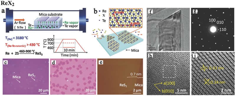
Figure 5.

a) Illustration of ReX2 (X = S, Se) growth modes via CVD method. The tellurium‐assisted CVD growth approach and b) the surface reaction approaches during epitaxial growth process of ReX2 atomic layer on mica. Optical images of monolayer ReS2 grown on c) mica substrate, d) after transferred onto SiO2/Si (300 nm) substrate. e) Atomic force microscope (AFM) image of as‐grown ReS2 on mica substrate. f) Low‐resolution TEM image of the ReS2 supported on a TEM grid. g) Selected area electron diffraction (SAED) patterns of the ReS2. h) High‐resolution TEM image of the ReS2. i) Fast Fourier‐transform (FFT) image of the marked area in (h). Reproduced with permission.62 Copyright 2016.
