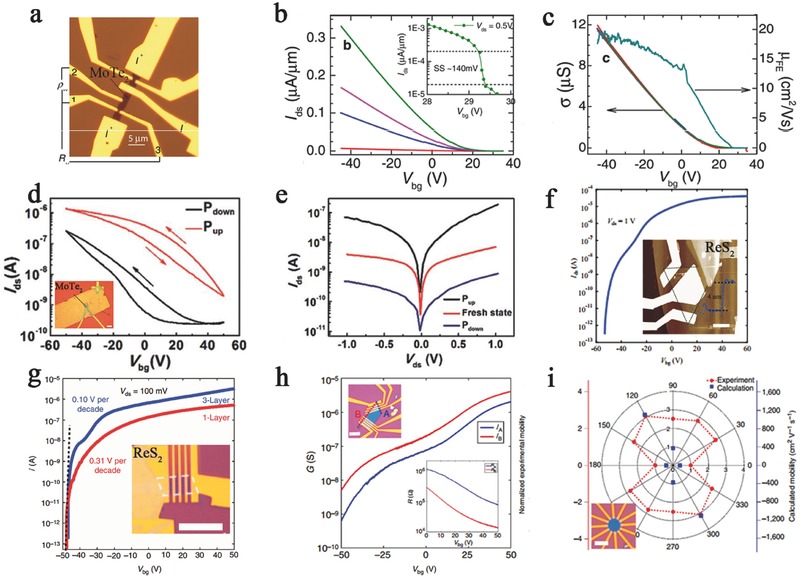
Figure 6.

a) Optical image of bilayered MoTe2‐based field‐effect transistors. b) The linear curves of I ds–V ds applied by different bias. The inset shows a subthreshold swing SS ≈140 mV, when I ds as a function of V bg in a limited scale. c) Conductivity (left axis) and mobility (right axis) as a function of V bg varied from 40 to −40 V. Reproduced with permission.167 Copyright 2014, American Chemical Society. d) The back‐gate transfer curves of MoTe2‐based phototransistors under the Pup state (red curve) and Pdown state (dark curve) of top gate fixing V ds at 1 V. Inset: Image of few‐layer MoTe2‐based FET with a ferroelectric polymer top gate. e) The output characteristics with fresh state (ferroelectric layer without polarization), Pup state, and Pdown state. Reproduced with permission.75 Copyright 2016, Royal Society of Chemistry. f) The transfer curve of a ReS2 transistor at a fixed V ds value of 1.0 V. Inset: AFM image of ReS2 device. Reproduced with permission.83 g) Transfer curves of monolayer (red) and trilayer (blue) ReS2 FET devices, when V ds is fixed at 100 mV. h) Transfer curves of anisotropic ReS2 FETs along A and B direction of a five‐layer flake (with an inner angle of 60° or 120°. Top inset shows optical image of the devices and the inset in the bottom performs the four‐probe resistance under V bg varying between 0 and 60 V. i) The calculated (red dots) and experimental (blue dots) mobility of monolayer ReS2 is plotted in the same graph, and the lowest mobility direction was set to be the 0° (or 180°) reference. Inset: The optical image of the device. Reproduced with permission.67 Copyright 2015, the authors, published under CC‐BY‐4.0 license.
