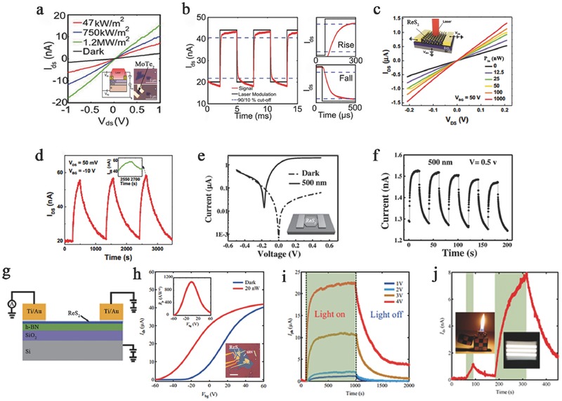
Figure 7.

a) The curves of V ds–I ds fixed at V g = 0 V under a different power of 685 nm laser. Inset: The schematic and two optical images of MoTe2 few‐layer FET. b) Photoresponse occurred in MoTe2 device at V ds = 5 V, V g = 0 V under a laser of 178 Hz and 20 µW. Zoomed region shows a rise time and a fall time. Reproduced with permission.22 c) Output characteristics of the curve of the ReS2 back‐gate device under different incident laser powers. Inset: The schematic structure of ReS2 photodetector. d) Photoresponse occurred with time‐dependent I ds of the device under an intermittent laser illumination. Inset: Enlarged image of the photoresponse peak over a small range. Reproduced with permission.115 e) The characteristic I–V curves were illuminated by light of the single ReS2 device. Inset: The schematic image of the device. f) Photoresponse occurred in ReS2 polycrystalline bilayer film with photocurrent under 500 nm incident light. Reproduced with permission.84 g) The schematic of the few‐layer ReS2 phototransistors. h) Linear transfer curves in the dark state and under illumination. Inset: Photoresponsivity as a function of V bg at the top and optical microscopy image and AFM image of the same device at the bottom. i) Photoswitching behaviors with high photoresponsivity under various V ds. j) Weak signal detection in a five‐layer ReS2 phototransistor, fixing V bg at −50 V and V ds at 2.0 V. Reproduced with permission.83
