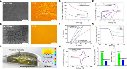
Fig. 2. Electrochemical and mechanical characterization of the device.

(A) Scanning electron microscopy (SEM) micrograph of O-Au (left) and optical micrograph of broken O-PB (right). (B) SEM micrograph of N-Au (left) and optical micrograph of complete N-PB (right). (C) Schematic of surface nanostructure–induced inner flow during ECD (left). Fluid mechanics simulation of the velocity distribution when the inner flow passes over the surface of the nanostructure (right, top) and electrochemical simulation of the growth rate of PB during ECD on N-Au (right, bottom). (D) Deposition current of O-PB (blue) and N-PB (red). (E) CV scan of O-PB (blue) and N-PB (red). (Inset) CV curve of O-PB (−0.05 to 0.35 V versus Ag/AgCl reference electrode at a scan rate of 50 mV/s). (F) Nyquist plot of EIS of O-Au (black), N-Au (red), O-PB (green), and N-PB (blue). (G) Response of N-PB to the same density H2O2 as a function of deposition time (that is, thickness). (H) CV of freshly deposited N-PB and N-PB after 2 months of storage. (I) Young’s modulus and hardness of N-PB (blue) and O-PB (green).
