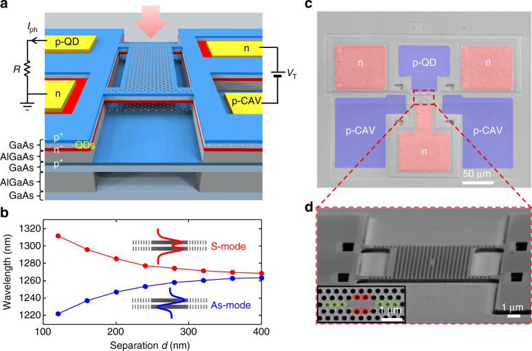
Fig. 1.
Overview of the sensor design. a Sketch of the device with electrical contacts and a visible cross-section with p- (blue) and n- (red) doped layers. QDs are located in the middle of the top membrane. Sensor actuation is possible by applying a reverse bias voltage (V T) to the tuning diode (on the right side), whereas the read-out is done by measuring the photocurrent from the photodiode (left side). b, Simulated optical mode wavelength dependence on the membrane separation for two modes that are symmetric (S) or antisymmetric (As) with respect to the out-of-plane direction. c False-colored SEM image of a typical device (top view) with contact pads to both sensing and actuation diodes. d Zoom-in SEM image showing the active part of the sensor: a four-arm bridge of dimensions 16 × 12 μm containing a photonic crystal cavity suspended above a fixed photonic crystal membrane. Inset: SEM image of the patterned L3 cavity design modified for high Q factor and large free-spectral range in a double-membrane structure. Optimization was done by displacing horizontally outwards and reducing the radius of six holes (green) and displacing four holes vertically (red)

