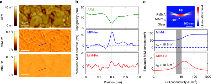
Fig. 4.
Various microstructures on the perovskite film. a AFM and MIM images showing the detailed features on the MAPbI3 thin film under 100 mW cm−2 illumination of the 532 nm laser. The photoresponse is uniform for grains with different heights and lateral sizes. All scale bars are 1 μm. b Line profiles across a single grain boundary (green in AFM, blue in MIM-Im, and red in MIM-Re) in a. The MIM contrast signals are referenced to the mean values on the grains. c Simulated MIM contrast, referenced to the background grain with a conductivity of 10 S m−1, as a function of the GB conductivity σ GB. The shaded column corresponds to the measured data within the experimental errors. The inset shows the simulated quasi-static displacement-field distribution for σ G = σ GB = 10 S m−1

