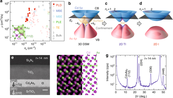
Fig. 1.
High-crystallinity and high-mobility Cd3As2 thin films. a Experimental trend of electron mobility versus sheet carrier density. Among our films (filled circle) prepared with pulsed laser deposition (PLD), high-quality ones obtained by high-temperature annealing are highlighted with bigger symbols. The mobility reaches a maximum of μ = 3 × 104 cm2/Vs even at a thickness of t = 30 nm, rivaling mobility values for bulk thinned plates (diamond22) and nanostructures (triangle23 and inverted triangle24), while it intrinsically decreases with reducing to two dimensions. Other films (circle) grown by molecular beam epitaxy (MBE)18,19, thermal evaporation (TE)15, or pulsed laser evaporation (PLE)16 techniques are also plotted for comparison. Inset shows the primary cubic structure of Cd3As2. b–d Schematic illustration of the electronic structure evolution from the 3D DSM state. With decreasing the film thickness, subbands are formed due to the quantum confinement, giving rise to two-dimensional topological insulating (2D TI) and trivial insulating (2D I) states depending on the number of inverted subbands6. e Cross-sectional image of a 14 nm Cd3As2 film sandwiched between Si3N4/TiO2 cap and SrTiO3 substrate. The length of the scale bar is 10 nm. f Atomically resolved element map of the boxed region in e, shown with the cross-sectional view of the crystal structure. g In the x-ray diffraction θ–2θ scan, Bragg peaks of the (112)-oriented Cd3As2 film are observed with clear Laue oscillations. The SrTiO3 substrate peaks are marked with an asterisk

