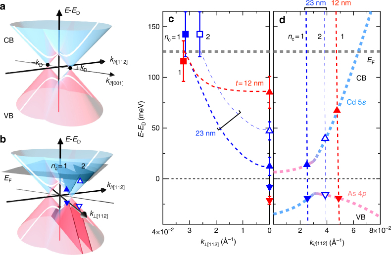
Fig. 4.
Electronic structures identified from quantum transport. a Cross sectional dispersions along the out-of-plane field direction (k ||[112]). b Subband formation (n c = 1 and 2) within the in-plane direction (k ⊥[112]), for t = 23 nm. c, d Constructed electronic structures measured from the Dirac point energy E D, are shown for the two typical thicknesses (t = 12 and 23 nm) (see Supplementary Fig. 13 for all the thicknesses). In c, the obtained Fermi energy E F and in-plane Fermi momentum k F are plotted for the split subbands (square). The bottom of the conduction band (CB) and the top of the valence band (VB) interpolated from previous calculations17 are indicated by an upward and a downward triangle, respectively. The error bars for E F were estimated from Eq. (1) by assigning effective mass values obtained using the Lifshitz-Kosevich formula for each filling state ν (see Fig. 3b). The structural plot in d represents the Bohr–Sommerfeld quantization condition along the film normal direction (Eqs. (2) and (3)), where the crossing point (triangle) of the original calculated band dispersions (dotted lines, left-hand side of Eq. (3))6 and the quantization condition curves (vertical dashed lines, right-hand side of Eq. (3)) determines the energy and momentum of the bottom of the split subbands. The orbital character of each subband is also identified, indicating the topological phase transition as represented by the color change of the subband (n c = 1) from blue (Cd 5s) to pink (As 4p). Subband data of n c = 1 (2) are distinguished by closed (open) symbols and thick (thin) dashed lines

