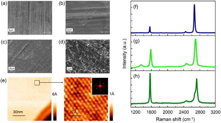
Figure 1.
Structural and morphological characterization of samples. SEM images of (a) NiF; (b) NiT; (c) FLG on Ni; (d) 4MLG on Ni; (e) Large-scale STM topography (100 × 100 nm2) of few-layers graphene grown on Ni (I = 0.7 nA, VBIAS = 0.1 V). High-magnification STM image (2.5 × 2.5 nm2) showing the triangular lattice atomic structure of few-layer graphene on Ni with lattice constant 2.4 Å, according to Fourier transform analysis (inset). Representative Raman spectra of SLG grown on Cu (for reference) (f), 4MLG tranferred on Ni (g) and FLG grown on Ni (h). Background caused by the luminescence of the copper was subtracted in the case of SLG grown and transferred on Cu.

