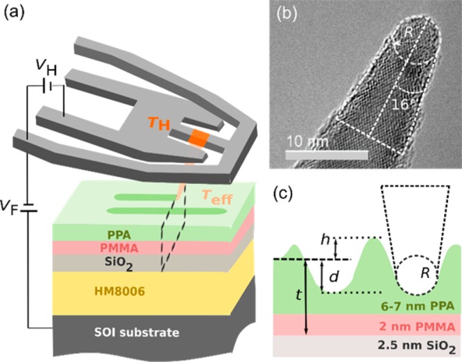
Figure 1.

(a) Schematic of the t-SPL patterning mechanism on the pattern transfer stack. The tip resting at a distance of 250 nm is heated to a temperature TH by applying the voltage VH to the resistive heater. A voltage VF is applied between the substrate and the cantilever to pull the tip into contact with the PPA surface for each patterning pixel. After contact, the polymer temperature is elevated to Teff < TH. (b) TEM image of an unused tip. The apex radius R is ∼3 nm. The estimated half-angle of the tip cone is 16°. (c) Schematic line shape profile for two consecutive lines. Between trenches of depth d a rim of height h is formed. The total thickness t of the polymeric PMMA and PPA layers is 8–9 nm.
