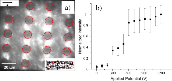
Figure 4.
DEP trapping of ssDNA-wrapped SWNTs. (a) IR fluorescence imaging of ssDNA-wrapped SWNTs subject to DEP trapping. At 700 Hz and 1000 V applied over the entire microchannel of 1.5 cm length, ssDNA-wrapped SWNTs accumulated in the regions of highest electric field strength, consistent with pDEP (scale bar, 20 μm; external field direction horizontal, along the x-direction). (b) Normalized fluorescence intensity indicative of DEP trapping vs applied electric potential for ssDNA-wrapped SWNTs in the regions where pDEP occurs. The onset of trapping was observed around 300 V, and above 600 V the fluorescence intensity reaches a plateau.

