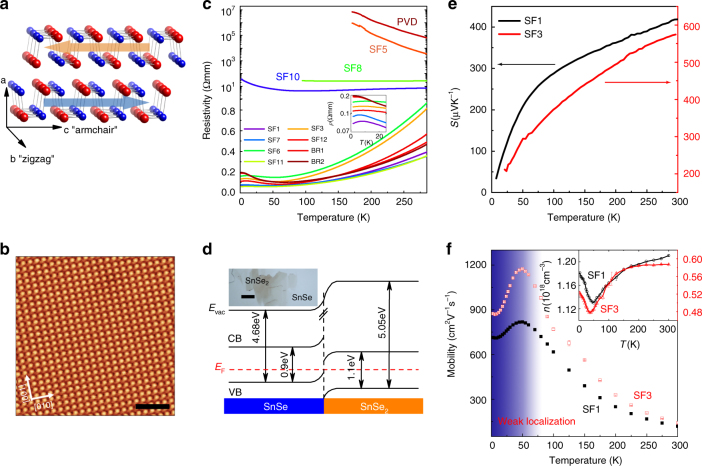
Fig. 1.
Characterisation of SnSe single crystals. a SnSe crystallises into the BP-type puckered bilayer structure, by forming alternating Sn- and Se-rows along the b-axis. The binary lattice is highly polarised with a net ferroelectric dipole field aligned with the c-axis. Here the red and blue balls represent Sn and Se atoms respectively. b Atomic-resolution nc-AFM image of stoichiometric SF1-SnSe, showing no existence of vacancies. The scale bar is 2 nm. c T-dependent ρ curves for all batches of crystals, showing various conduction behaviour from metallic (SF1, SF3, SF6, SF7, SF11, SF12, BR1, and BR2) to semiconducting (SF5, SF8, SF10, and PVD). Below 50 K, all metallic batches exhibit upturns in ρ vs T curves, a manifestation of WL. The inset zooms in the ρ vs T curves below 30 K. d Energy level alignment of SnSe/SnSe2 heterostructure. Interfacial charge transfer leads to p-doping in SnSe. Note that the exact value of E F depends on both the concentration and thickness of SnSe2 microdomains. The inset is a typical optical image of SnSe2 microdomains on SnSe. The scale bar is 10 μm. e High S b of SF1- and SF3-SnSe, which are in agreement with the literature reports. f T-dependent Hall measurements of SF1- and SF3-SnSe reveal mobility enhancement at low T, which is typical metallic behaviour. Note that the mobility drops below 50 K is due to WL

