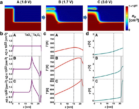
Fig. 11.

Simulation results for the reset transition of the device. a Vo density (nD) map. Calculated profiles of b nD, c T, and d y for states A (1.0 V), B (1.7 V), and C (3.0 V). The position of z = 15 nm indicates the Ta2O5/TaOx interface in the structure schematic. The shaded area shows the depleted gap, defined for nD < 5 × 1021 cm-3 [87]
